


상품이 준비중입니다.


Ambient-pressure Photoemission Spectroscopy Systems
(대기압 광전자 방출 측정 시스템)
| Description | ||||||||
|---|---|---|---|---|---|---|---|---|
|
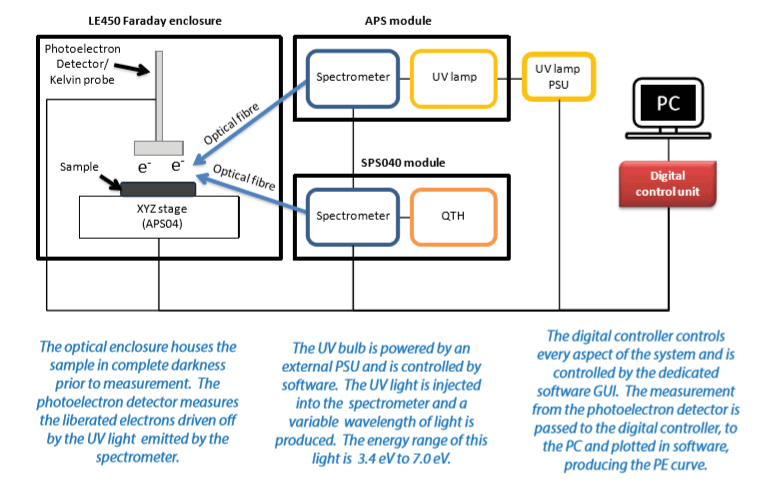
The Ambient-pressure Photoemission Spectroscopy (APS) systems are one of KP Technology Ltd’s most recent additions to our large surface analysis range. Domestic and international patents are held for these instruments. APS measures the absolute work function (Φ) of a material by photoemission in ambient conditions, no vacuum is required. The excitation range of APS is 3.4 eV to over 7.0 eV, meaning that APS is capable of measuring the absolute work function of metals and the ionization potential of semiconductors alongside measurement of the surface Fermi level with the Kelvin probe.
|
|
|||||||
| Features | Applications | |||||||
| • Work function measurement by photoemission in air | • Organic and non-organic semiconductors | |||||||
| • Density of states measurements | • Metals and metal alloys | |||||||
| • 3.4 eV to 7.0 eV energy range | • Thin Films and surface oxides | |||||||
| • Measurement of all semiconductor bands | • Corrosion and nanotechnology | |||||||
| • Contact potential difference by Kelvin probe | • Solar cells and organic photovoltaics | |||||||
| Measurement Principle | ||||||||
|
When light is incident on a material such as a metal or a semiconductor, the photons may have enough energy to liberate electrons from the surface, a process known as the Photoelectric Effect.
The energy required for electrons to escape the material is termed the work function. By varying the energy of the incoming light, the absolute work function can be established.
|
 |
|||||||
 |
||||||||
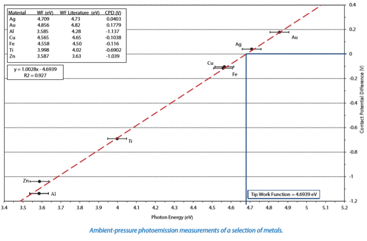
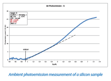
| Each metal was measured with the photoemission mode and Kelvin probe mode of an APS02 system. The contact potential difference (CPD) was measured with the Kelvin probe and the work function was measured by the ambient pressure photoemission mode. When work function is plotted against CPD, a straight line is formed. A line is drawn at 0 V CPD to the line and when traced down reveals the absolute work function of the tip. | ||||||||
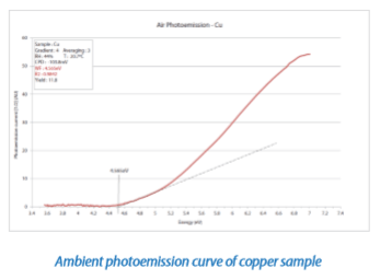
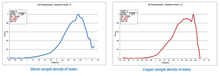
| Density of States | ||||||||
| The properties of many materials are governed by the Density of States (DOS) near the Fermi level. The Ambient-pressure Photoemission system is capable of probing the DOS by differentiating the detected photoelectron yield with respect to the incident photon energy. The DOS measurement can thus be compared to molecular orbital calculations for the material under investigation. DOS data collected with the APS in air is shown to the right for copper. The data for all measured samples is consistent with literature. | ||||||||
 |
||||||||
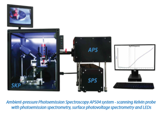
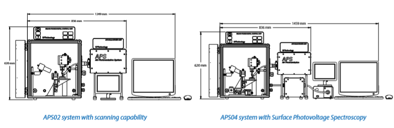
| System Overview | ||||||||
 |
||||||||
| System Specifications | APS01 | APS02 | APS03 | APS04 | ||||
| Kelvin probe 3-axis scanning | V | V | V | |||||
| Surface Photovoltage | V | V | ||||||
| Surface Photovoltage Spectroscopy | V | |||||||
| Tip material / diameter | 2 mm gold tip | |||||||
| CPD resolution | 1-3 meV | |||||||
| Height control (Auto) | 25 mm automatic | |||||||
| Kelvin probe mode and PE mode | CPD and photoemission measurements | |||||||
| CPD measurement time | CPD measurements in | |||||||
| PE resolution | Full photoemission measurement | |||||||
| WF measurement time | PE measurement in | |||||||
| DOS measurements | Full access to DOS information | |||||||
| Optical system | Colour camera with zoom lens and monitor for positioning | |||||||
| Oscilloscope | Digital TFT oscilloscope for real-time signal | |||||||
| Test sample | Gold, aluminum and silver test samples | |||||||
| Faraday enclosure base | 450 x 450 mm | |||||||
 |
||||||||
상품정보에 배송/교환/반품 및 취소와 관련된 안내가 별도 기재된 경우 ,아래의 내용보다 우선하여 적용됩니다.
-
상호명(주)프로브스
-
대표자김용균
-
사업자등록번호215-87-50331
-
통신판매업번호제2017-서울송파-1811호
-
대표전화070-7836-5319
-
팩스전화02-6280-5319
-
이메일이메일: probes.ykkim@gmail.com
-
개인정보취급책임자김용균, 호스팅업체: 원데이넷,
-
사업장소재지서울특별시 송파구 법원로 90, 파트너스 2, 503호
-
지정택배사
-
기본배송비배송비 5,000원 (100,000원 이상 무료배송)
-
평균배송기간배송등록 후 2-3일
-
반송주소서울특별시 송파구 법원로 90, 503호(문정동 파트너스2)
- 제품 하자의 경우 전화로 해당 건에 대해 설명과 함께 하자에 대한 내용을 메일로 사진과 함께 남겨주십시오.
- 제품 하자 이외 단순 변심에 의한 교환/반품은 불가합니다.
- 제품 수령 후 제품의 이상 유무를 7일 이내 확인해 주십시오.
- 반품/교환 요청기간이 지난 경우
- 구매자의 책임 있는 사유로 상품 등이 멸실 또는 훼손된 경우 (단, 상품의 내용을 확인하기 위하여 포장 등을 훼손한 경우는 제외)
- 구매자의 사용 또는 일부 소비에 의하여 상품의 가치가 현저히 감소한 경우
- 오랜 시간의 경과로 제품의 이상 유무를 확인하기 어려운 경우
- [공지사항] AFM 측정 자료실 오픈2021-08-06
- 창립 10주년 감사 이벤트2021-02-05
고객센터
070-7836-5319
09:00 ~ 18:00
주말 및 공휴일은 휴무입니다.
Email : probes.ykkim@gmail.com
입금계좌[신한은행]전화문의 후 번호확인(주)프로브스