")


상품이 준비중입니다.


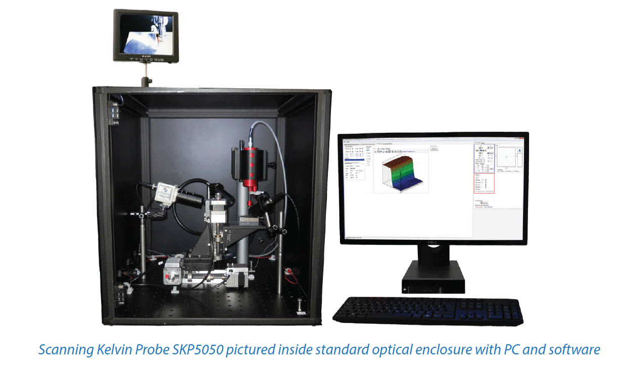
Scanning Kelvin Probe System
(3D 켈빈 프로브)
| Description | |||||||
|---|---|---|---|---|---|---|---|
|
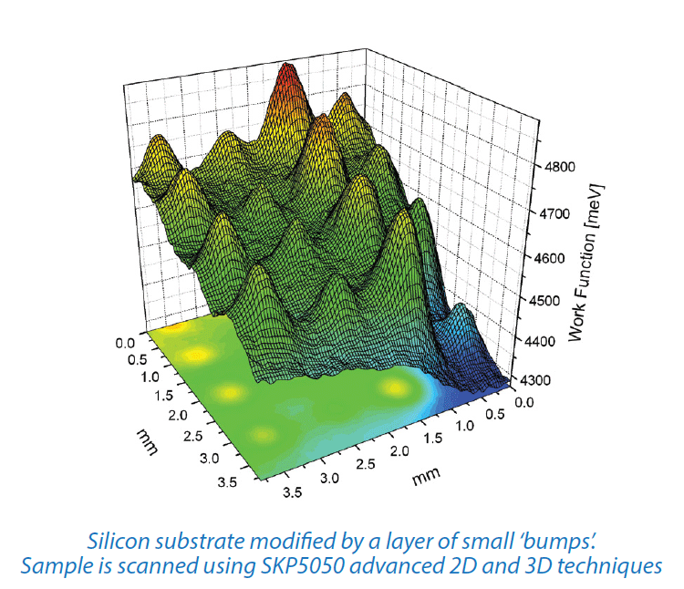
Our large range of Scanning Kelvin Probes give the user full access to 2D and 3D work function plots of samples ranging in size from 50 mm to 350 mm. With work function resolution of 1-3 meV, and the spatial resolution of the probe tip diameter, the Scanning Kelvin Probe gives reliable, repeatable measurements for work function (φ), contact potential di erence (CPD) and Volta potential (Δψ) measurements.
Effects of corrosion can be measured across a surface with high precision e.g. coating uniformity and performance. A Faraday and optical enclosure shields all of our scanning systems from unwanted fast changing environmental conditions, electromagnetic interference and provides the perfect platform for our Ambient Pressure Photoemission Spectroscopy (APS) and Surface Photovoltage add-on modules. |
|
||||||
| Features | Applications | ||||||
| • Work function measurement by Kelvin probe | • Organic and non-organic semiconductors | ||||||
| • Work function resolution of 1-3 meV | • Metals and metal alloys | ||||||
| • Scanning area from 50mm to 350mm | • Thin Films and surface oxides | ||||||
| • Scanning resolutio equal to tip diameter | • Solar cells and organic photovoltaics | ||||||
| • Autoumatic height regulation | • Corrosion and Nanotechnology | ||||||
| • Tip diameter 2.00mm or 0.05mm (SKP5050) | • Quality control | ||||||
| Specifications | SKP5050 | ASKP350350 | |||||
| • Tip material / diameter | Standard 2mm gold tip | ||||||
| • Work function resolution | 1-3 meV | ||||||
| • Sample scan size | 50mm x 50mm | 350mm x 350mm | |||||
| • Probe translation | 25mm (Auto) | 50mm(Auto) | |||||
| • 3D sample area | Square | Square & Circular | |||||
| • Visualisation | 3D maps of surface potential | ||||||
| • Oscilloscope | Digital TFT oscilloscope for real time signal | ||||||
| • Test sample | Godl / Al sample | ||||||
| • Control Supplied | PC control with dedicated software for full digital control of all parameters | ||||||
| • Detection system | Off-null with parasitic capacity rejection | ||||||
| • Faraday Enclosure | 450mm x 450mm | 450mm x 600mm | |||||
| • Optical system | Colour camera with zoom lns and monitor | ||||||
| Upgrades and Add-Ons | |||||||
| • Ambient Pressure Phtoemission Spectroscopy (APS) | 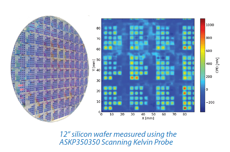 |
||||||
| • Surface Photovoltage Spectroscopy (400-1000nm) | |||||||
| • Surface Photovoltage (QTH or LED) | |||||||
| • Sample heater to 250°C | |||||||
| • Relative humidity control and notroge environmental chamber | |||||||
| • Tips in gold or stainless steel : 0.05mm to 2.00mm | |||||||
상품정보에 배송/교환/반품 및 취소와 관련된 안내가 별도 기재된 경우 ,아래의 내용보다 우선하여 적용됩니다.
-
상호명(주)프로브스
-
대표자김용균
-
사업자등록번호215-87-50331
-
통신판매업번호제2017-서울송파-1811호
-
대표전화070-7836-5319
-
팩스전화02-6280-5319
-
이메일이메일: probes.ykkim@gmail.com
-
개인정보취급책임자김용균, 호스팅업체: 원데이넷,
-
사업장소재지서울특별시 송파구 법원로 90, 파트너스 2, 503호
-
지정택배사
-
기본배송비배송비 5,000원 (100,000원 이상 무료배송)
-
평균배송기간배송등록 후 2-3일
-
반송주소서울특별시 송파구 법원로 90, 503호(문정동 파트너스2)
- 제품 하자의 경우 전화로 해당 건에 대해 설명과 함께 하자에 대한 내용을 메일로 사진과 함께 남겨주십시오.
- 제품 하자 이외 단순 변심에 의한 교환/반품은 불가합니다.
- 제품 수령 후 제품의 이상 유무를 7일 이내 확인해 주십시오.
- 반품/교환 요청기간이 지난 경우
- 구매자의 책임 있는 사유로 상품 등이 멸실 또는 훼손된 경우 (단, 상품의 내용을 확인하기 위하여 포장 등을 훼손한 경우는 제외)
- 구매자의 사용 또는 일부 소비에 의하여 상품의 가치가 현저히 감소한 경우
- 오랜 시간의 경과로 제품의 이상 유무를 확인하기 어려운 경우
- [공지사항] AFM 측정 자료실 오픈2021-08-06
- 창립 10주년 감사 이벤트2021-02-05
고객센터
070-7836-5319
09:00 ~ 18:00
주말 및 공휴일은 휴무입니다.
Email : probes.ykkim@gmail.com
입금계좌[신한은행]전화문의 후 번호확인(주)프로브스